Identifying Coil Symbols and Layout on Schematic Diagram.
The symbol of a coil (inductor) is just like a wave lines which emphasized that there is a winding component on that circuit which means that the coil is connected in there. In cellphone circuit many coil is being used in B+ voltage filtering to avoid saturated voltage and current.
coils are easy to identify in an schematic diagram for they are form into a wave line. It is labeled with letter "L" which means Inductance.
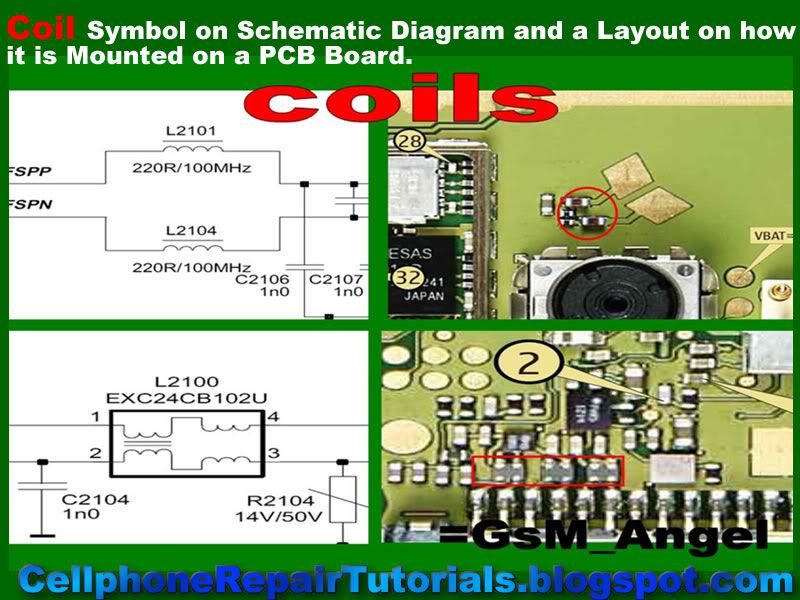
In cellphone circuit coils are also prone to be easily damaged like when it is being used in B+ line filtering. It will be blown out or end up busted if some short circuit occurs.
Identifying Integrated Circuit Symbols and Layout
Integrated circuits, also called "chips", are electronic circuits where all the components (transistors, diodes, resistors and capacitors) has been manufactured in the surface of a thin substrate of semiconductor material.
Integrated circuit is designed to save extra space on modern electronics.
In electronics, an integrated circuit (also known as IC, microcircuit, microchip, silicon chip, or chip) is a miniaturized electronic circuit (consisting mainly of semiconductor devices, as well as passive components) that has been manufactured in the surface of a thin substrate of semiconductor material. Integrated circuits are used in almost all electronic equipment in use today and have revolutionized the world of electronics.
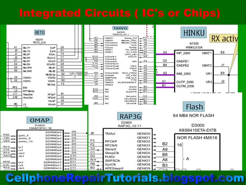
In mobile phones it is packed with each desired certain applications purpose like
Power Management, Baseband Processor, Application Processor , Memory Storage, Audio Codecs, Bluetooth and Wi-Fi Ciruits.
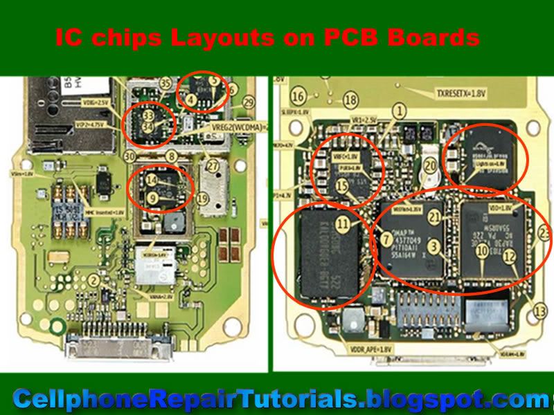
Some large pack chips composed of many circuits and certain application both in-place in one packaging.
IC Chips are very delicate to handle with and troubleshoot if found faulty, it needs a little bit deep knowledge and understanding on how that chips works on a particular circuit. Experience is the best tool to handle with it.
Identifying DC to DC Voltage Drivers, Regulators and Converters Symbols and Layout
DC to DC Regulators and Converters are packed in a tiny BGA (ball grid array) chips.
It used to convert, regulate and drives a certain amount of current-voltage.
It has the ability to stabilize, reduce or step up a voltage that feeds towards it.
in mobile phones it has a digital signal that been able to switch it on and off.
like for example it switch the LED lamp that used to light up the Display Screen while the cellphone is in used status and turn it off when the cellphone is not in use or at the sleep mode.
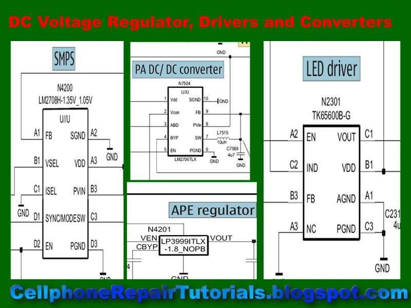
There are various kind and designed of these said components which according to each every purpose to the circuit. Sizes and bumps leads also have may differ with each other.
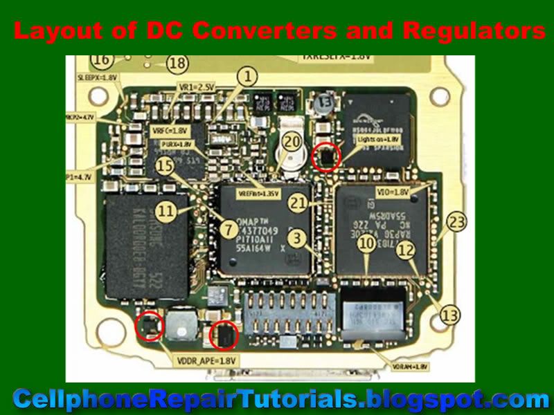
This chips may also damaged cause by a corrosive element or if a short circuit occurs.
Identifying EMI-ESD Symbols and Layout on schematic diagram and PCB board
EMI-Electromagnetic Interference and ESD-Electrostatic Discharge is pack in tiny chips called by many technician as Crystal IC for it glows like a crystal glass.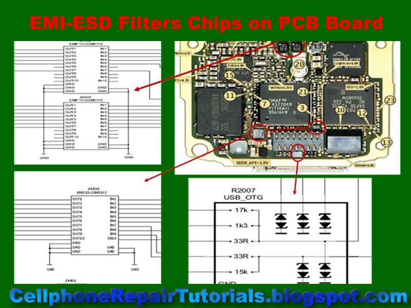
EMI-ESD filter are used to protect a certain circuit from hazardous Electromagnetic Interference and Electrostatic Discharge.
Electromagnetic Interference cause by elecromagnetic machines like like a chainsaw, an electric blower and other things that has high frequency levels.
Electrostatic Discharge (ESD)- a human body is a potential source of electrostatic and can cause damage, especially to semiconductor devices when touching it.
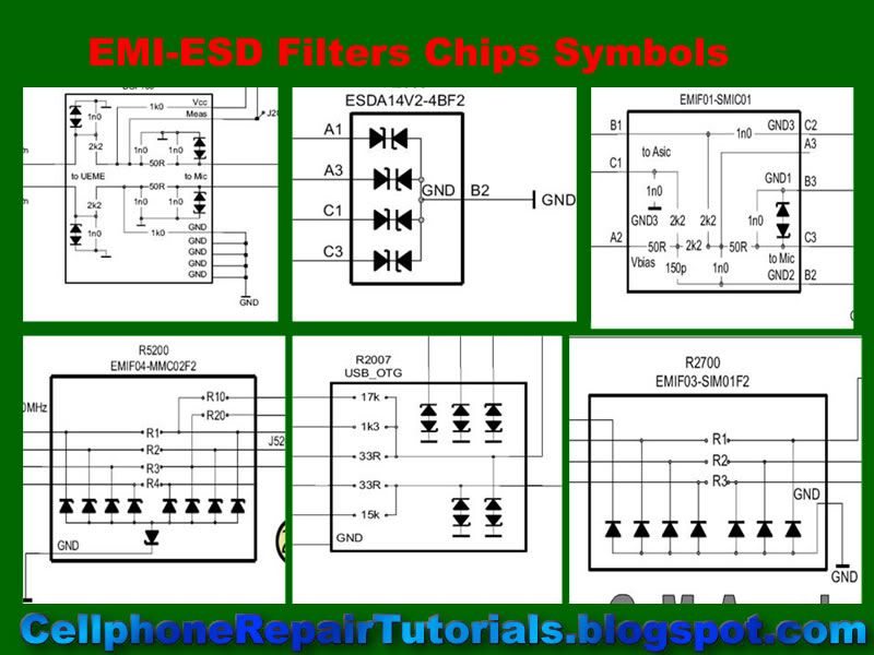
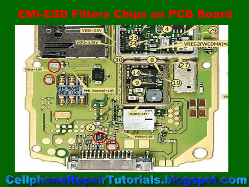
EMI-ESD Filters can be easily breakdown and busted when those two elements occurs. It often used in Keypads circuit, Display circuit, USB (Universal Serial Bus)Interface circuit, Removable Flash Memory Devices circuit and other Interface that is prone to ESD and EMI hazards.
EMI-Electromagnetic Interference and ESD-Electrostatic Discharge is pack in tiny chips called by many technician as Crystal IC for it glows like a crystal glass.

EMI-ESD filter are used to protect a certain circuit from hazardous Electromagnetic Interference and Electrostatic Discharge.
Electromagnetic Interference cause by elecromagnetic machines like like a chainsaw, an electric blower and other things that has high frequency levels.
Electrostatic Discharge (ESD)- a human body is a potential source of electrostatic and can cause damage, especially to semiconductor devices when touching it.


EMI-ESD Filters can be easily breakdown and busted when those two elements occurs. It often used in Keypads circuit, Display circuit, USB (Universal Serial Bus)Interface circuit, Removable Flash Memory Devices circuit and other Interface that is prone to ESD and EMI hazards.
Identifying RF Filter Symbols and Layout
RF filters of all types are required in a variety of applications from audio to RF and across the whole spectrum of frequencies. As such RF filters form an important element within a variety of scenarios, enabling the required frequencies to be passed through the circuit, while rejecting those that are not needed.
The ideal filter, whether it is a low pass, high pass, or band pass filter will exhibit no loss within the pass band, i.e. the frequencies below the cut off frequency. Then above this frequency in what is termed the stop band the filter will reject all signals.
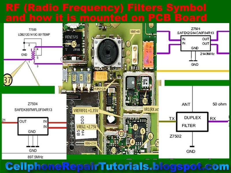
Basic types of RF filter
There are four types of filter that can be defined. Each different type rejects or accepts signals in a different way, and by using the correct type of RF filter it is possible to accept the required signals and reject those that are not wanted.
The four basic types of RF filter are:
* Low pass filter
* High pass filter
* Band pass filter
* Band reject filter
As the names of these types of RF filter indicate, a low pass filter only allows frequencies below what is termed the cut off frequency through. This can also be thought of as a high reject filter as it rejects high frequencies. Similarly a high pass filter only allows signals through above the cut off frequency and rejects those below the cut off frequency. A band pass filter allows frequencies through within a given pass band. Finally the band reject filter rejects signals within a certain band. It can be particularly useful for rejecting a particular unwanted signal or set of signals falling within a given bandwidth.
Identifying Battery Cell Symbols and Layout
A back up battery cell or button cell is being used in cellphones circuit to back up the digital clock crystal oscillator. It used to maintain the clock at its real time status.
Its like when removing the battery of the mobile phone wont reset the settings of the digital clock that is being installed on a phone. Some phones without battery back-up like the old ones need to reset again after removing and replacing the battery. Its a big help to a digital circuits such high tech mobile phones circuit.
A battery cell is have two lead terminal which is negative and positive voltage output.
The metal can case of this type of battery is its positive (+) terminal, and the negative (-) terminal is the cap.
The negative is connected to a ground lines of a circuit while the positive is feed to a clock oscillator circuit. It has low power output voltage range from 1.5 volts to 3.5 volts. In mobile phones used about 3.3voltage output.
They are compact and have long life. They are usually a primary single cell with a nominal voltage between 1.5 and 3 volts. Common anode materials are zinc or lithium. Common cathode materials are manganese dioxide, silver oxide, carbon monofluoride, cupric oxide or oxygen from the air. Mercuric oxide batteries were formerly a common battery type but have been withdrawn from marketing due to their mercury content.
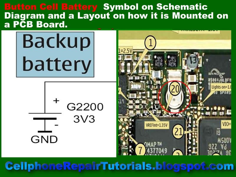
A back up battery may also damaged when due to degradation, corrosion and losses its voltage when being shorted or by liquids like water;
A damaged battery cell can be easily notice when a leakage occurs, its liquid chemical will flow out and can cause damages to a nearby components.
In a mobile phones you can determine when the back-up battery is weak, when try to set the time of the clock, then power it off and by removing the battery for a while and put it back again, when the clock stayed at its time where you set, it means that back-up battery is still working but, if it ask you to set the clock again it means that the back-up battery is not working.
Identifying Battery Cell Symbols and Layout
A back up battery cell or button cell is being used in cellphones circuit to back up the digital clock crystal oscillator. It used to maintain the clock at its real time status.
Its like when removing the battery of the mobile phone wont reset the settings of the digital clock that is being installed on a phone. Some phones without battery back-up like the old ones need to reset again after removing and replacing the battery. Its a big help to a digital circuits such high tech mobile phones circuit.
A battery cell is have two lead terminal which is negative and positive voltage output.
The metal can case of this type of battery is its positive (+) terminal, and the negative (-) terminal is the cap.
The negative is connected to a ground lines of a circuit while the positive is feed to a clock oscillator circuit. It has low power output voltage range from 1.5 volts to 3.5 volts. In mobile phones used about 3.3voltage output.
They are compact and have long life. They are usually a primary single cell with a nominal voltage between 1.5 and 3 volts. Common anode materials are zinc or lithium. Common cathode materials are manganese dioxide, silver oxide, carbon monofluoride, cupric oxide or oxygen from the air. Mercuric oxide batteries were formerly a common battery type but have been withdrawn from marketing due to their mercury content.
A back up battery may also damaged when due to degradation, corrosion and losses its voltage when being shorted or by liquids like water;
A damaged battery cell can be easily notice when a leakage occurs, its liquid chemical will flow out and can cause damages to a nearby components.
In a mobile phones you can determine when the back-up battery is weak, when try to set the time of the clock, then power it off and by removing the battery for a while and put it back again, when the clock stayed at its time where you set, it means that back-up battery is still working but, if it ask you to set the clock again it means that the back-up battery is not working.Identifying User Interfaces Components such as Power Switch, Microphone, Earpiece and Ring-tone speakers and Layouts On Schematic Diagram
User Interface Components are those components
such as power switch, keypads,vibrator , a micro phone such asmouthpiece, speakers like earpiece and ring tones speaker. These components are also important to familiarized with , for these are commonly prone to be easily got damaged. when it comes to hardware troubleshooting, in Nokia service manual or Schematic diagram it is marked for easy guides while some other various mobile phone products was not.
In the symbols below the power switch labeled as power key, and also likewise the keypad component symbols that is a circle with two pointing lines insides labeled as keyboard.

In mobile phones there is one microphone and two micro speakers being used; First is the microphone that receive the voice to transmit,

the two micro speakers are examples on the picture below,

the first one is for the hearing which is called the earpiece, that is the one that send the voice to hear, the second one is for the ring-tones speaker, it is that send the tones and tell that someone is calling or sending a message. Familiarizing the uses and works of these three micro speakers on a circuit is a big help for troubleshooting.
Identifying Clock Crystal Oscillator Symbols and Layout
Oscillator
An electronic component circuit that have the ability create real time clock signal. a vibrating crystal that made by so-called piezoelectric material produce a maintained and sustained frequency such as applied into real time clock like quartz wristwatches.. This one is being used to maintain the clock system in a digital circuit and maintain Radio Frequency transmitters and Receivers.
It labeled sleep clock oscillator or just clock oscillator in schematic diagrams.
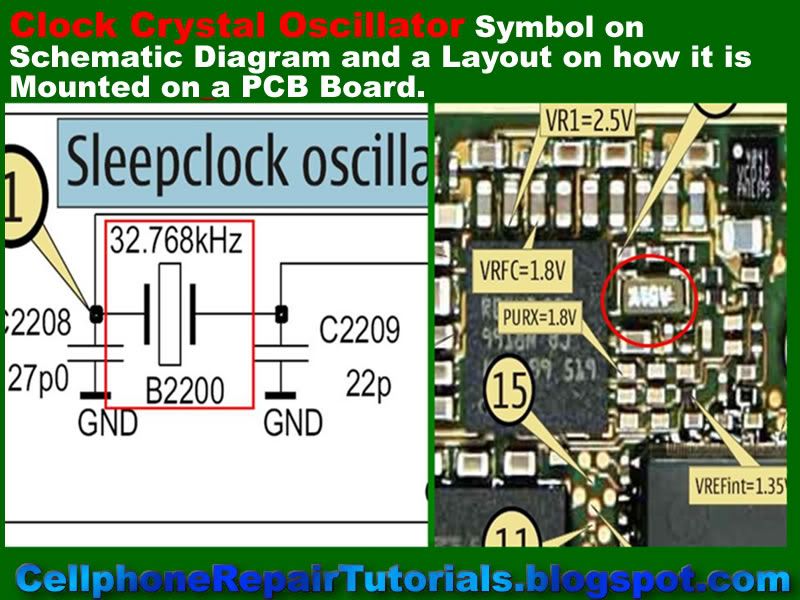
In Cellphones if the clock oscillator is faulty it results on not powering the phone. The phone is dead, because as stated above that oscillator supports on digital radio frequencies circuitry.
Identifying Fuse Symbols and Layout
Fuse
A fuse is the component used to protect from sudden arise of the desired amount of currents and voltages into a certain circuit. The fuse will be blown out if a certain circuit have a very low resistance or shorted. a Fuseo is made by a metal wire that can be easily busted if a high current or voltage will flow on it.
It is labeled letter "F" means a fusible device then a product code or number.

A fuse is often used in a charging circuit of any mobile phones. The phone will indicate no charging reaction if a fuse is already blown.
How to Find Component Parts on PCB Board?
A certain components parts is easy to find with an aide of schematic diagrams. In Nokia Phones finding it was been so easy for they provide a complete and accurate component data on their Schematic Diagrams. While other various mobile phone don't have. Some cellphone technicians find it hard to fix some of mobile phone products for they don't provide schematic diagrams to be available, but many experts and masters can do the job even without schematic diagrams. Experts can rely on their deep knowledge on electronics components and circuits, many of them where electronic engineers and also many of them where professionally skilled by experience and mastered for years. You can be one of them if you follow their instinct but before that they all started from scratch.We are all start from scratch.
Now, let's take up a very simple method on how to find certain electronic component's location where it is being mounted on a particular PCB Board layouts.
Here's an example of Nokia N70 schematic diagram, Download it here if you haven't a copy yet, and make sure you have Adobe Reader installed on your computer to be able to open it.
If you already have a copy of this schematic diagram, open it and scroll it down to the bottom page.
In the bottom page which is the last page you may found this Component Finder Page. see picture below:
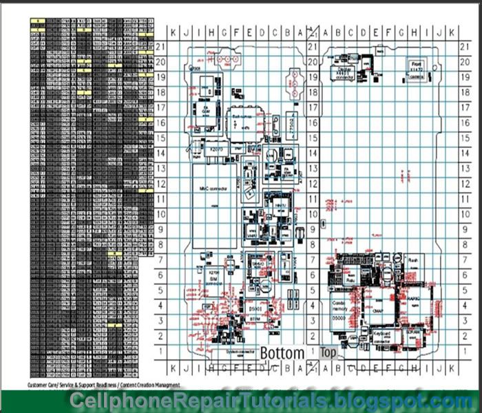
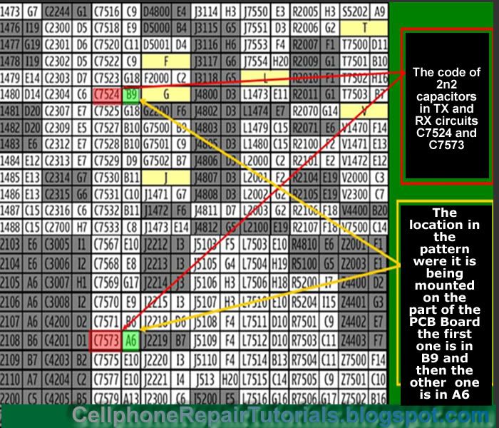
On the right side you may find the table of components which is listed in codes like for example, Resistors starts with letter "R" then "mounting code" . next to it on the left is the "pattern codes" which is means the spot point which is scaled by letters and numbers on the PC Board,
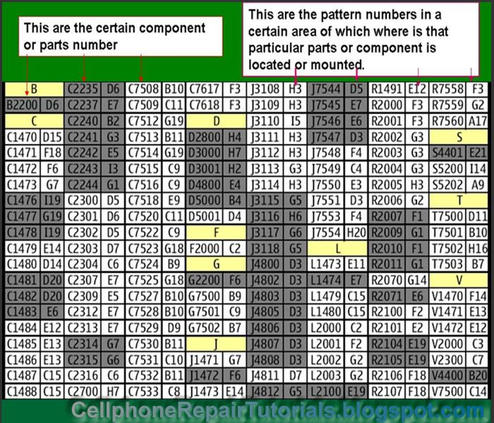
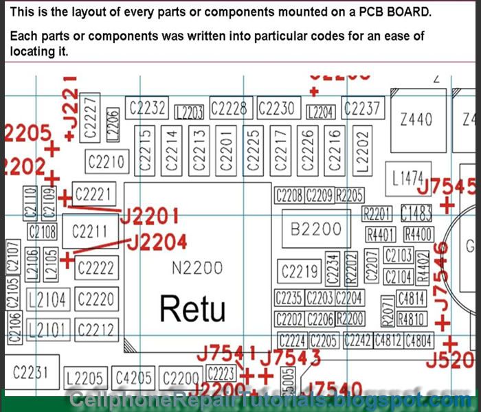
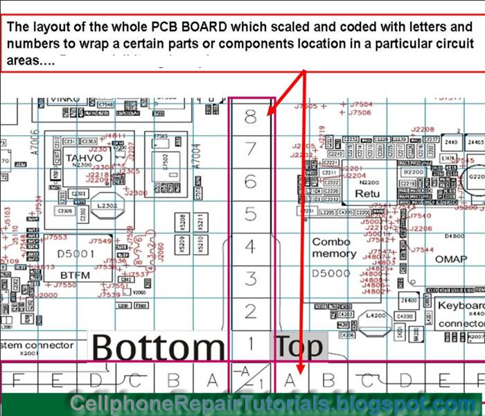
On the right side of the page is the layout of all of components with respectivecodes mark on it. Each component mounted in horizontal and vertical positions.
In both sides on the PCB layout is being scaled by letters and numbers, this is were the pattern codes from the first picture above being produce by combining the letter and number to make the mapping spot point.
The spot point of where these letter and number meets across each other, is the exact location where that certain component is being mounted.
Now let's take a little bit exercise on how to use this methods..
Okay, assuming that we are looking for a certain components on a PCB board.
Let say that we are going to find the 2n2 valued capacitor on RF Section for that phone is having a problem of network signal.
now scroll up the page to RF Section which is on page 9 and find these two 2n2 (2.2nanofarad) valued capacitor see guide picture below; Just remember and get the Mounting Code for it is the code were going to use as a guide to to the component finder table of components.
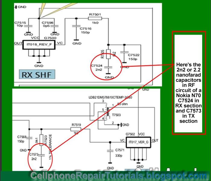
Then after finding it scroll back to the Component Finder page Table of components, then find it on the lists of the components codes like "C7524 is on B9" and "C7573 is on A6"
the next thing again you have to do is to remember and get that code then proceed to the Component Layouts. and scale the spot point of "letter B and 9" then letter "A and 6" on the scaled on the opposite sides.See picture below
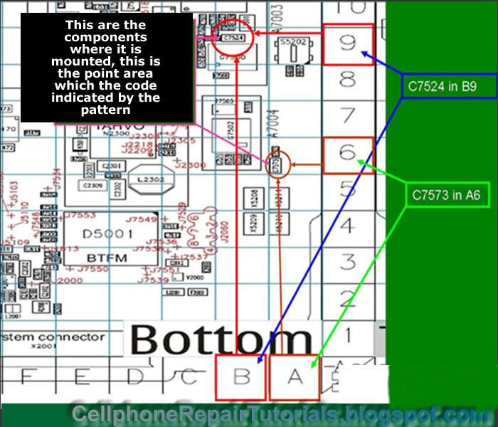
The last part is to scroll it up on the whole component layout on the upper page 10 or on your PC board then spot and mark that component where it is being mounted.
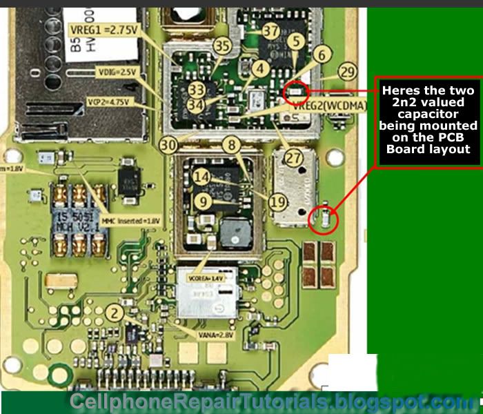
There you go you just found it! congratulation!
Practice it more often,so that you can be familiarize on each component or parts for that certain product. The more often you do it, the more chances you will mastered it. sooner,you can work it alone without even using the schematic diagram anymore.
A certain components parts is easy to find with an aide of schematic diagrams. In Nokia Phones finding it was been so easy for they provide a complete and accurate component data on their Schematic Diagrams. While other various mobile phone don't have. Some cellphone technicians find it hard to fix some of mobile phone products for they don't provide schematic diagrams to be available, but many experts and masters can do the job even without schematic diagrams. Experts can rely on their deep knowledge on electronics components and circuits, many of them where electronic engineers and also many of them where professionally skilled by experience and mastered for years. You can be one of them if you follow their instinct but before that they all started from scratch.We are all start from scratch.
Now, let's take up a very simple method on how to find certain electronic component's location where it is being mounted on a particular PCB Board layouts.
Here's an example of Nokia N70 schematic diagram, Download it here if you haven't a copy yet, and make sure you have Adobe Reader installed on your computer to be able to open it.
If you already have a copy of this schematic diagram, open it and scroll it down to the bottom page.
In the bottom page which is the last page you may found this Component Finder Page. see picture below:

On the right side you may find the table of components which is listed in codes like for example, Resistors starts with letter "R" then "mounting code" . next to it on the left is the "pattern codes" which is means the spot point which is scaled by letters and numbers on the PC Board,

On the right side of the page is the layout of all of components with respectivecodes mark on it. Each component mounted in horizontal and vertical positions.

In both sides on the PCB layout is being scaled by letters and numbers, this is were the pattern codes from the first picture above being produce by combining the letter and number to make the mapping spot point.
The spot point of where these letter and number meets across each other, is the exact location where that certain component is being mounted.

Now let's take a little bit exercise on how to use this methods..
Okay, assuming that we are looking for a certain components on a PCB board.
Let say that we are going to find the 2n2 valued capacitor on RF Section for that phone is having a problem of network signal.
now scroll up the page to RF Section which is on page 9 and find these two 2n2 (2.2nanofarad) valued capacitor see guide picture below; Just remember and get the Mounting Code for it is the code were going to use as a guide to to the component finder table of components.

Then after finding it scroll back to the Component Finder page Table of components, then find it on the lists of the components codes like "C7524 is on B9" and "C7573 is on A6"

the next thing again you have to do is to remember and get that code then proceed to the Component Layouts. and scale the spot point of "letter B and 9" then letter "A and 6" on the scaled on the opposite sides.See picture below

The last part is to scroll it up on the whole component layout on the upper page 10 or on your PC board then spot and mark that component where it is being mounted.

There you go you just found it! congratulation!
Practice it more often,so that you can be familiarize on each component or parts for that certain product. The more often you do it, the more chances you will mastered it. sooner,you can work it alone without even using the schematic diagram anymore.
hello I need help for reading schematic mobile phone and means short code
ReplyDeletethanks very good I need method reading schematic
ReplyDelete