Understanding the Keypad circuit may help and boost your knowledge on fixing keypad problem issues on mobile phones. Keypads is a part of user interface being used to navigate or enter numbers, letters and characters, browse application, sends information and etc.
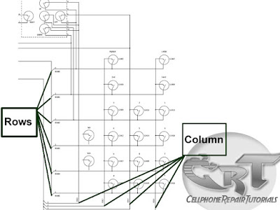
An schematic diagram below will help us understand how keypad circuits works and which components or parts did this circuit is being connected.
In this diagram the each and every key switching pads is being divided and grouped into rows and columns. Each rows and columns were group into 2 -5 keypads switch. This rows and columns have each corresponding lines according to each and every group of switching pads.
This lines of rows and columns is being filtered for EMI and ESD protection the EMI filter is made of tiny chip that used to protect such EMI and ESD interference.
This rows and columns lines are digital switching signals generated by the application processor to trigger or activate every corresponding digital datas that is being stored and programmed within the mobile phone system memory. This diagram below is an Application Processor that generates and feeds then receives digital data switching signals.
This digital data frequency signals corresponds and interpreted to each key characters that are marked on each keypads. Like for example a combination of row 2 and column 3 will triggered the number 3 when hitting on it.
this block diagram below shows how the switching signal is being triggered to process a command data.
Various mobile phones have different keypads layouts and specification. A joystick and a volume switch is also parts of keypads switching circuits. Some keypads module designs are made into a flexible wire like those Slide Type package of mobile phones. Some flexible wires are very vulnerable and common cause of keypad malfunction. There are few methods in tracing and mapping the keypad layout on a mobile phones keypads on printed circuit board. One of this quick and very easy method is by using an schematic diagram, if that certain mobile phones have available unto it. Schematic diagram is very useful guide in every aspects of hardware troubleshooting.
Now assuming that you already have knowledge how to use and read it, follow this simple steps below.
Browse to bottom of the pages where yo can locate and find like the picture below., it is the keypad circuit section. In that schematic layout you will notice that each corresponding key characters is being group into lines. This group of keypad switch lines is being marked with rows and columns.
Practice this kind of method with an aide of schematic diagram, in this way if you're skills grows further, you can then trace any other mobile phones without any schematic diagram available at first hand.


Thanks for this amazing post, I found some interesting information about membrane keypad….! Keep up posting Really helpful – thanks for sharing these! !
ReplyDeleteGracias por la información
ReplyDelete